Philco 46-480 Electronic Restoration
Posts: 287
Threads: 16
Joined: Jan 2024
City: Tulsa
State, Province, Country: Oklahoma
I should also make two more comments. First, the diameter of this PCB is 1.45", to match the diameter of the multi-section capacitor I am replacing. The QC connectors I am using for the twist lock connectors are positioned exactly where they will pass through the cutouts in the chassis. And second, all clearances and creepage distances are in excess ofthe 3mm design constraint. Hence why there are no cutouts or notches in the PCB. I believe the smallest distance measured was 5 mm.
Joseph
Philco 46-480
Philco 49-906
Posts: 16,501
Threads: 572
Joined: Oct 2011
City: Jackson
State, Province, Country: NJ
With 450V on separate, especially the opposite layers you simply do not have to worry about breakdown. Not with 62 mils, not with 31 mil....
Looks good.
I would beef up the caps' pads sizes. Also, if you have tall caps, and you also have the tabs that could be twisted, using teardrops makes sense.
People who do not drink, do not smoke, do not eat red meat will one day feel really stupid lying there and dying from nothing.
Posts: 287
Threads: 16
Joined: Jan 2024
City: Tulsa
State, Province, Country: Oklahoma
What are teardrops? Is that a style of capacitor?
Joseph
Philco 46-480
Philco 49-906
Posts: 16,501
Threads: 572
Joined: Oct 2011
City: Jackson
State, Province, Country: NJ
No. Teardrops is a style of a trace entry into a pad.
https://www.pcbway.com/blog/PCB_Basic_In...166ec.html
People who do not drink, do not smoke, do not eat red meat will one day feel really stupid lying there and dying from nothing.
Posts: 287
Threads: 16
Joined: Jan 2024
City: Tulsa
State, Province, Country: Oklahoma
Okay, yes. I’m familiar with the concept but knew it as a fillet. Let me make the modifications. You raise a good idea.
Joseph
Philco 46-480
Philco 49-906
Posts: 16,501
Threads: 572
Joined: Oct 2011
City: Jackson
State, Province, Country: NJ
Yes, fillet is another name for teardrops, or, rather, one of the type of it. The most popular one.
Teardrops will not be generated if the trace enters into the pad not radially, or if the entry segment is short.
Most CADs will generate them automatically if the option is enabled.
People who do not drink, do not smoke, do not eat red meat will one day feel really stupid lying there and dying from nothing.
Posts: 287
Threads: 16
Joined: Jan 2024
City: Tulsa
State, Province, Country: Oklahoma
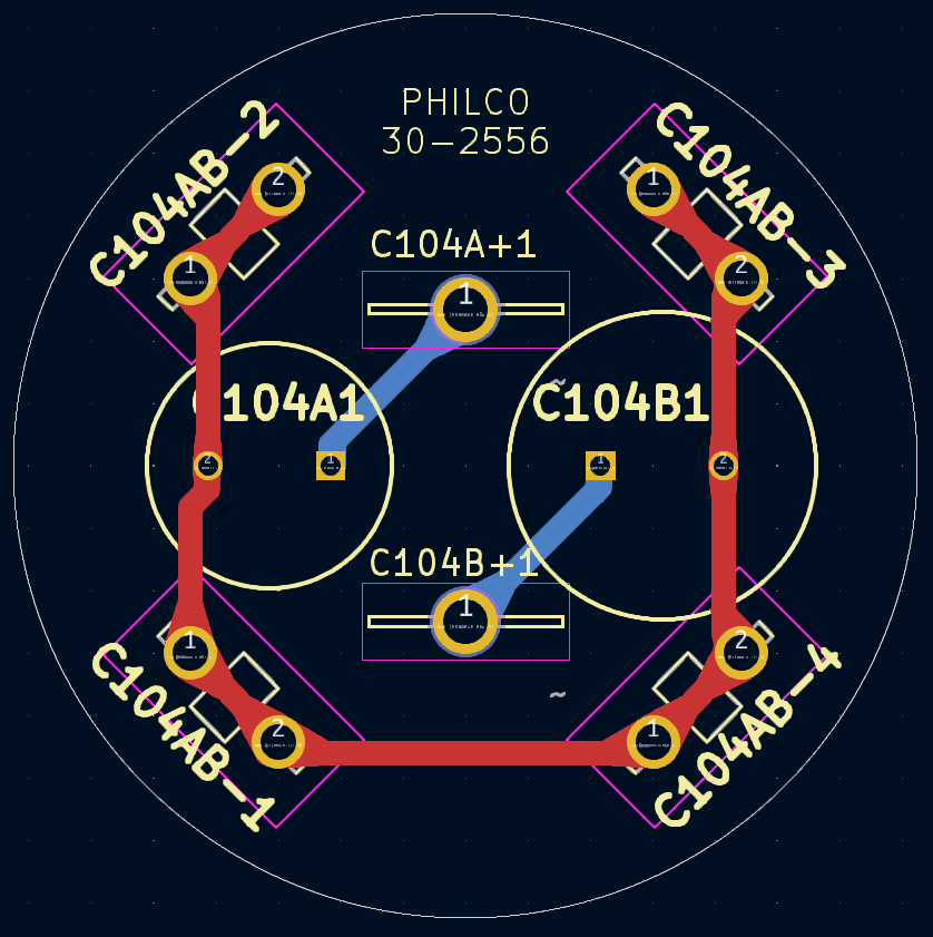
Here we are. Not too difficult at all!
Joseph
Philco 46-480
Philco 49-906
Posts: 16,501
Threads: 572
Joined: Oct 2011
City: Jackson
State, Province, Country: NJ
BTA, the trick to add a teardrop to a pad that is not directly on the way of your 45 degree trace (your square pads) is to break the trace in the middle and zig-zag to another 45 degree trace that noaw has the target pad on its way.
(Or, in case you do not mind using non-45 degree angles, just to go to "any angle" routing mode and draw a direct trace between the two pads).
People who do not drink, do not smoke, do not eat red meat will one day feel really stupid lying there and dying from nothing.
Posts: 287
Threads: 16
Joined: Jan 2024
City: Tulsa
State, Province, Country: Oklahoma
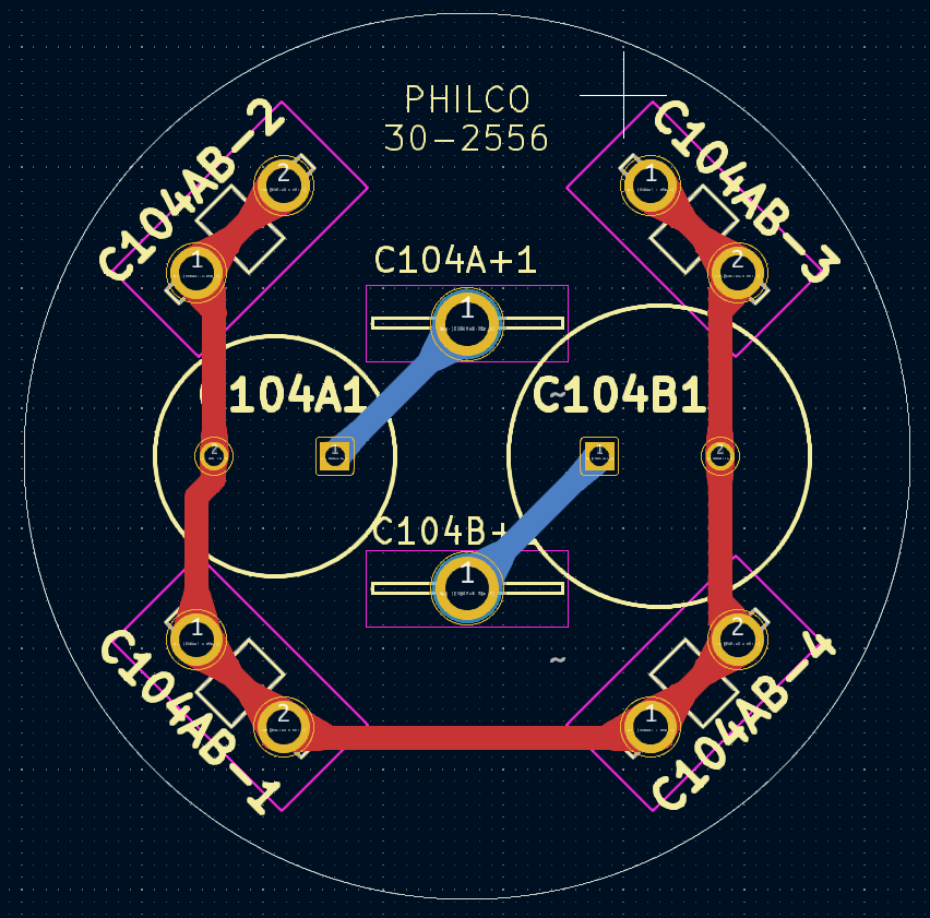
Here we are, I was able to relocate the solder lug connectors to be precisely 45 degrees from the respective terminal on each capacitor. Clearances are still at 5mm, which exceeds the 3mm minimum.
Joseph
Philco 46-480
Philco 49-906
Posts: 16,501
Threads: 572
Joined: Oct 2011
City: Jackson
State, Province, Country: NJ
It always looks more colorful in CAD than on the PCB 
SInce I do not know the dimensions of your solder lugs/tabd, make sure they are not to close to the caps' barrels and will not rub against it.
Also, personally, with high voltages I try to run the traces (if they cross the aluminym can outline) on the opposite side to the one the caps are mounted on. I honestly do not know what the insulation property of that film that covers the caps.
People who do not drink, do not smoke, do not eat red meat will one day feel really stupid lying there and dying from nothing.
Posts: 287
Threads: 16
Joined: Jan 2024
City: Tulsa
State, Province, Country: Oklahoma
Luckily my plan is for those solder lugs to be on the underside of the PCB, whereas the capacitors will be on the top side. Even so, I know that the through-hole connector will protrude just a bit through the top. I measured, and there should be 3.4mm of clearance between the connector and the edge of the capacitor. Great consideration!
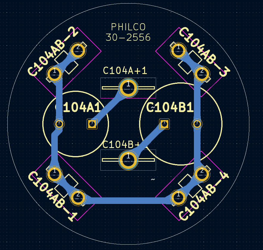
As for the comment about the high voltage traces, I hadn't considered this. You clearly have a lot of experience designing PCBs. I welcome all of these comments! Lets fix this by placing all traces on the bottom layer. All traces will be on the opposite side of the PCB compared to the capacitors. The traces connecting to the negative contacts will be equipotential with the chassis, so it wouldn't matter if the solder mask were scraped and the trace contacted the chassis. Additionally, the two positive contacts could not possibly touch the chassis as they are located in the area of the cutout in the chassis.
Joseph
Philco 46-480
Philco 49-906
Posts: 16,501
Threads: 572
Joined: Oct 2011
City: Jackson
State, Province, Country: NJ
Yep.
It always help to put some sort of keepout outline, which is not necessarily the "keepout" keepout, but just some outline denoting the area where certain things should not enter.
Could be on a mechanical layer, so it does not show up in the artwork.
In this case it's the cutout you've mentioned.
It immediately visualizes the relation of the cutout and the traces/pads/outlines etc.
People who do not drink, do not smoke, do not eat red meat will one day feel really stupid lying there and dying from nothing.
Posts: 287
Threads: 16
Joined: Jan 2024
City: Tulsa
State, Province, Country: Oklahoma
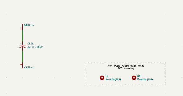
I started this morning on the design for a PCB for C101. The original component is a single-section electrolytic capacitor mounted on a phenolic wafer. C101 is a 22 µF, 450 VDC, 20% capacitor. I began with the schematic. Again, KiCAD is strange because you have to add any mounting holes to the schematic. But here it is.
I am using the same solder lugs as I used for C104 A/B, so I imported the same footprint library. I also was able to get this capacitor's footprint from Mouser's website. I paired footprints to schematic symbols, and then started with the PCB design. I borrowed the shape of this PCB from the design I created for my 49-906 multi-section capacitor. I utilized the tips Mike provided for my C104 A/B capacitor, and applied them here (traces on the opposite side of the PCB if they cross the edge of the capacitor's can, adding teardrops to the through-hole mounts, etc.). I've also used the same clearance, creepage, and ampacity assumptions I made for C104 A/B. My traces are 1mm wide and I'm assuming a minimum clearance and creepage of 3mm. All clearances and creepages for through-hole connectors and traces are acceptable on this board. I also temporarily inserted a ring to represent the circle cutout on the chassis. All connectors are at least 3mm away from the cutout, so there will be no clearance issues with the chassis. The only comment I will make is that the capacitor's can is not 3mm away from the upper edge of the PCB. I simply did not have enough space on this PCB to make that happen. However, we are not assuming that the body of the capacitor is energized. Here's a snapshot of this PCB.
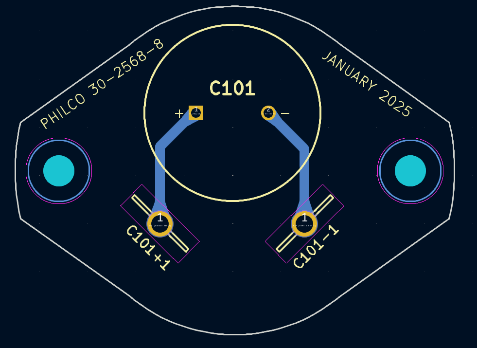
I added the date to this PCB. I had forgotten to add that to the PCB for C104 A/B, but I will do that now. It will help me remember 15 years from now that it's time to recap this radio!
Joseph
Philco 46-480
Philco 49-906
Posts: 16,501
Threads: 572
Joined: Oct 2011
City: Jackson
State, Province, Country: NJ
Many CADs are this way.
You do not have to add non-electrical items to the sch, like MTHOLEs, fiducials, etc, but as long as they are footprints and therefore are components, when re-annotating the sch to the PCB, they may get deleted.
You could lock (freeze, glue - the terminology varies between CADs) them, but it all depends on a specific CAD. KiCad accepts holes both as drills/pads and board outlines patterns inside the main outline.
Cap's can should be OK as it still has an insulating film, which accounts for some dielectric strength and, together with air gap should do fine. The can in todays caps is not an electrode, but should not be ignored either. Especially if running hi-V traces under it.
People who do not drink, do not smoke, do not eat red meat will one day feel really stupid lying there and dying from nothing.
Posts: 1,858
Threads: 119
Joined: May 2008
City: Omak
State, Province, Country: WA
Hello Joseph,
Wow very nice work what program are you using to draw this in ?
That is too funny " added the date to this PCB. I had forgotten to add that to the PCB for C104 A/B, but I will do that now. It will help me remember 15 years from now that it's time to recap this radio!"
I restored my Philco 610b like in 2004 or 5 and just this last year I replaced the Sprague Atom Capacitors with Film type since one of them was going bad .
Sincerely Richard
Users browsing this thread: 2 Guest(s)
|
|
Recent Posts
|
|
The list of my radio & TV collection!
|
| Peter;
I can't say for certain but many North American made radios from that era, the late 1940s onward, had silver m...Arran — 02:06 AM |
|
Philco 39-7C Restore
|
| A little more work today. I got the first IF transformer back together after replacing the wiring going to the 78 tube ...klondike98 — 12:06 AM |
|
Two small radios from France. Restoration and review.
|
| And here they are, the French beauties ready:
In summary, the suspicion that radio transmits the national cha...Vlad95 — 10:46 PM |
|
Two small radios from France. Restoration and review.
|
| One is ready for washing, the other for painting:
ATTENTION
Faint-hearted and heart patients,
please d...Vlad95 — 10:36 PM |
|
Two small radios from France. Restoration and review.
|
| Range Switch Block:
I thought that mica capacitors of this type died out in the 30s, but no, they just moved ...Vlad95 — 10:29 PM |
|
Two small radios from France. Restoration and review.
|
| Chassis bottom view:
Again, like twins, especially in the range switch part.
Front panels:
And...Vlad95 — 10:25 PM |
|
Two small radios from France. Restoration and review.
|
| Chassis removed, front view:
Chassis rear view:
It will be enough for the first device to prescribe a bath.
Bu...Vlad95 — 10:11 PM |
|
Two small radios from France. Restoration and review.
|
| France
Peculiarities of national character.
Excelsior-52 threw me off track. It was too far outside my established...Vlad95 — 10:06 PM |
|
Philco 16b no shortwave reception
|
| First let thank everyone who helped ID this radio a few weeks ago!
I have replaced all the capacitors and was able to r...Ken D. — 08:07 PM |
|
Philco model 38 code 121 not receiving signal.
|
| Ah yes, the Philco "Green Death" strikes again, someone suspected that cellulose nitrate based insulation migh...Arran — 06:23 PM |
|
Who's Online
|
| There are currently no members online. |

|
 
|


![[-] [-]](https://philcoradio.com/phorum/images/bootbb/collapse.png)


