01-01-2025, 08:06 PM
Good afternoon, folks! I've gotten a lot covered since I last provided an update. First, I created a separate post to ask about replacing the power transformer. Per the advice of many others, I was encouraged to salvage the original unit. It worked perfectly after some cleanup, repainting, and sleeving the cables.
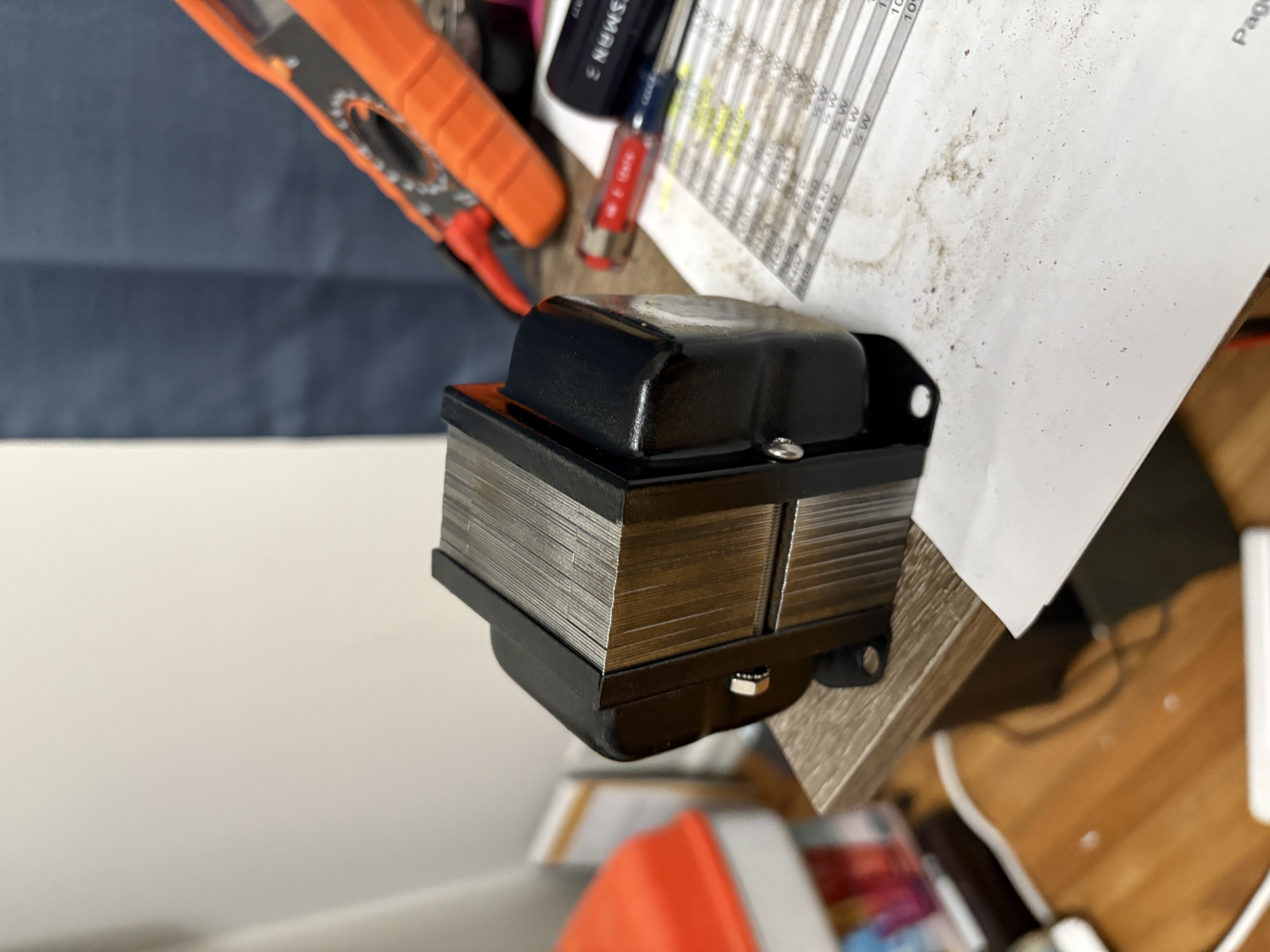
Next, I began combing through the chassis to verify the circuit. I was able to make MANY corrections to my schematic. I had noted in one of the earlier posts that I wasn't able to read some of the pin numbers on the wafer switches for band selection from the Philco schematic, so I have now gotten those corrected. I also corrected a few wire crossings on my schematic--sometimes I couldn't tell from the Philco schematic if two overlapping wires formed a node or not, so I had to give it my best guess. I corrected three of them that I had gotten wrong.
I have an answer to another discrepancy I noted earlier. I showed two screenshots, one from the overall schematic on page 113 of the documentation and another from a Section 4 schematic on page 109 of the documentation. The overall schematic did not depict a grid resistor connecting to pin 8 of the 7F8, whereas the other schematic did. I have confirmed that there is a 10-ohm resistor, per the section 4 schematic. Thus, I have added it into my schematic.
I have also determined the production run of this radio. There were eight listed production runs for the main chassis and nine production runs for the RF chassis in the Philco documentation. This particular chassis has the modifications indicated for production run 8 of the main chassis and production run 9 of the RF chassis, so it was among the last of the 46-480's to ever be manufactured. I've also determined that three capacitors have been replaced at some point or other, but the work was done very cleanly. The guy from whom I bought this radio mentioned that he "inherited" it when his father passed away. He said that his father was a collector of older radios, and he didn't want to throw them all away.
It took me a very long time to make my way through the RF chassis. The reason is that there is a complex assembly of four double-sided wafer switches for the band selection, and most of the components are woven around and in between the wafers. I have no good way to convey this in words, so here are a few photos.
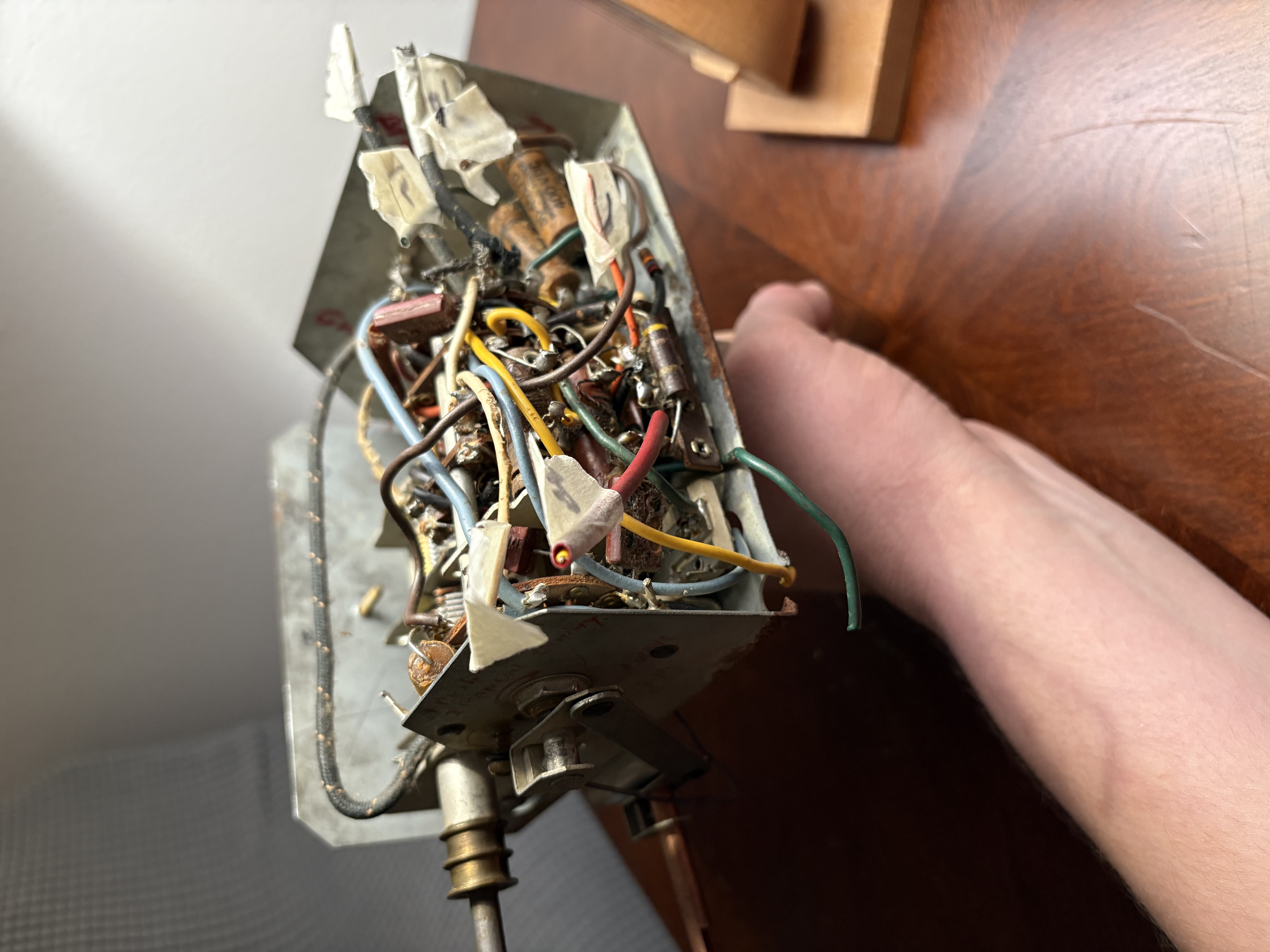
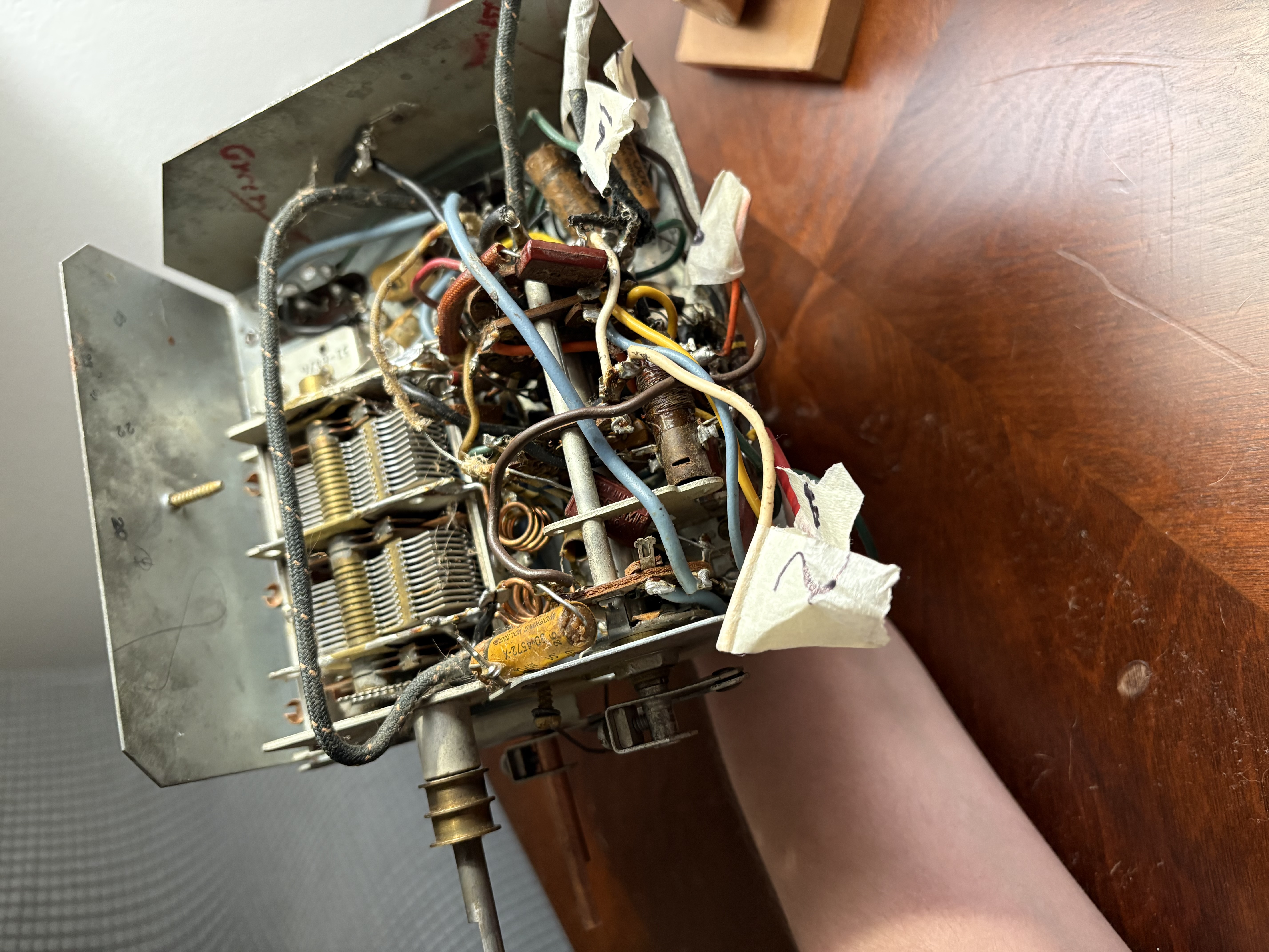
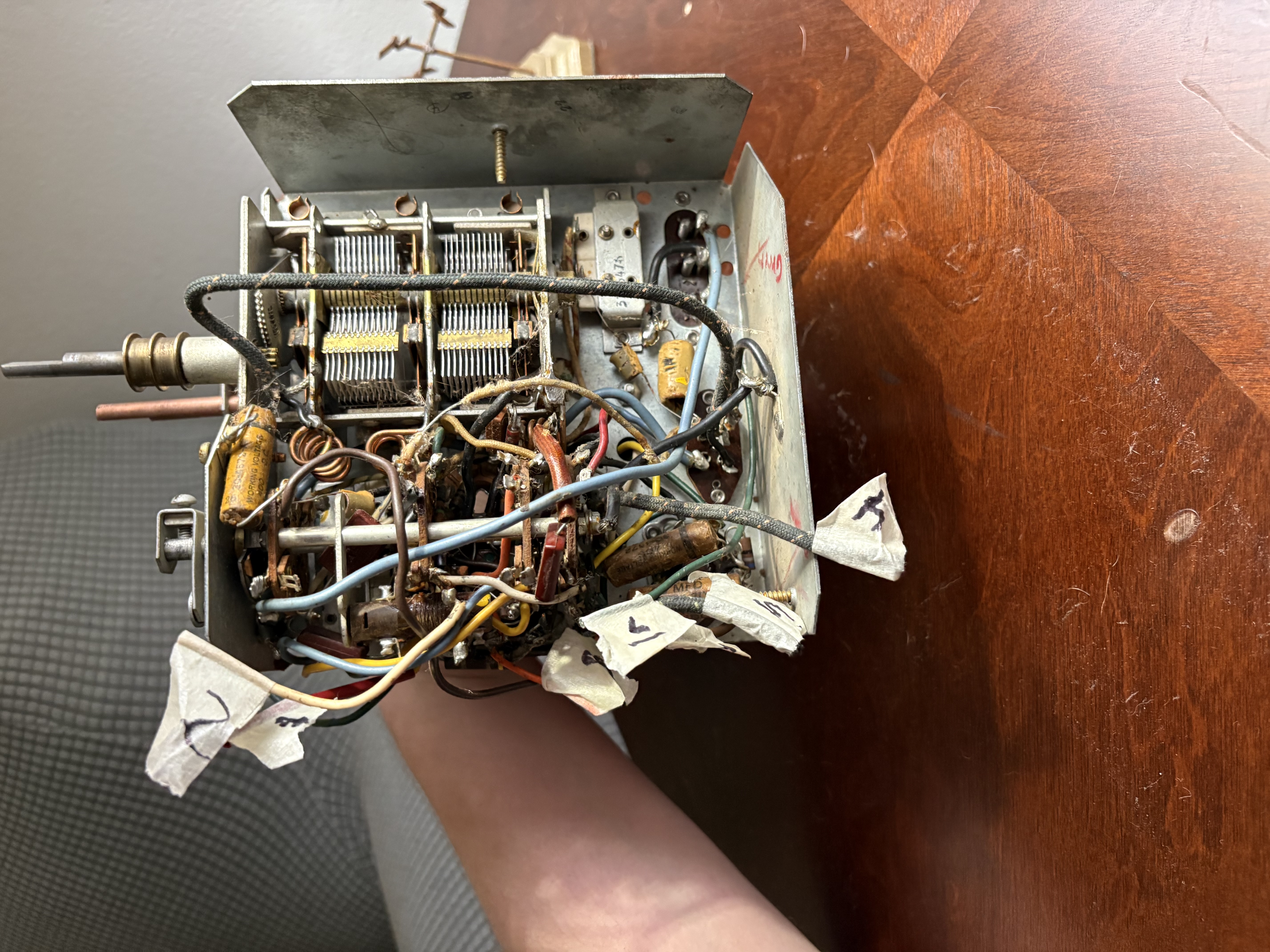
I dread rewiring this portion, because it is VERY densely packed. This assembly is also obstructing the underside of the 7F8 socket and the underside of the C404A/B/C trimmer caps. But I know that I will have to rebuild it, because there is evidence of mice having chewed on a few of the cables which connect to this wafer switch assembly. There's also two paper capacitors embedded into the assembly that I need to replace, and a mica capacitor that I can see with a broken lead.
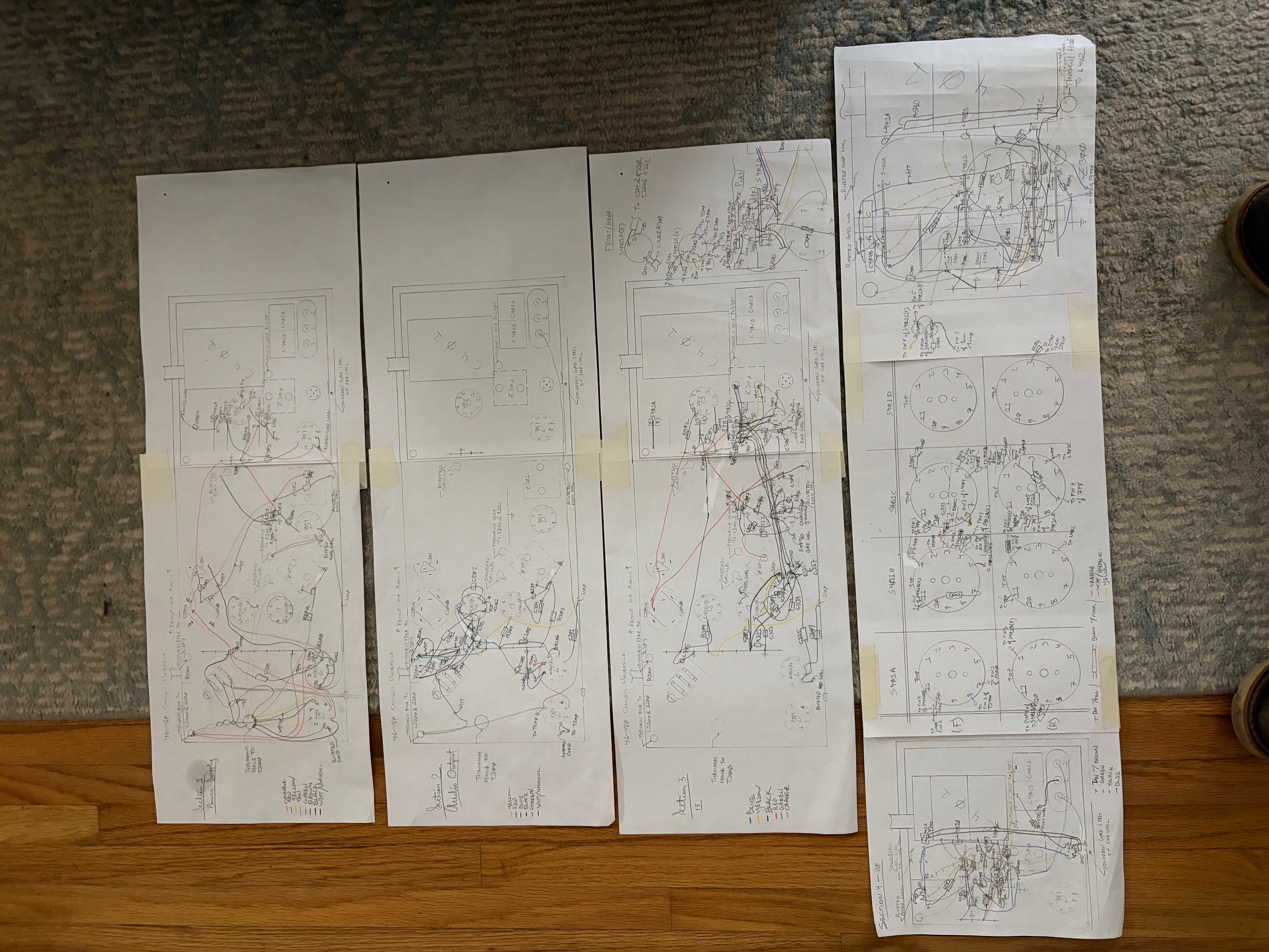
As I made my way through the circuit, I've created drawings to depict the physical wiring. I created four drawings--one for each section of the schematic. I know that I will have to do a fair amount of disassembly to get this chassis cleaned and all of the components repaired/replaced, so I needed to make sure that I exactly how everything is placed.
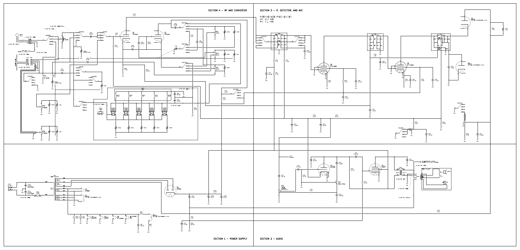
At this point I have confirmed the values of about half of the resistors and only a few of the capacitors. Many of them I need to get to as I remove them in order to see the color codes. I will update my schematic with corrections to the values if I find any during disassembly. I've attached the schematic as it currently stands, both here as an image and as a PDF attachment.
Next, I began combing through the chassis to verify the circuit. I was able to make MANY corrections to my schematic. I had noted in one of the earlier posts that I wasn't able to read some of the pin numbers on the wafer switches for band selection from the Philco schematic, so I have now gotten those corrected. I also corrected a few wire crossings on my schematic--sometimes I couldn't tell from the Philco schematic if two overlapping wires formed a node or not, so I had to give it my best guess. I corrected three of them that I had gotten wrong.
I have an answer to another discrepancy I noted earlier. I showed two screenshots, one from the overall schematic on page 113 of the documentation and another from a Section 4 schematic on page 109 of the documentation. The overall schematic did not depict a grid resistor connecting to pin 8 of the 7F8, whereas the other schematic did. I have confirmed that there is a 10-ohm resistor, per the section 4 schematic. Thus, I have added it into my schematic.
I have also determined the production run of this radio. There were eight listed production runs for the main chassis and nine production runs for the RF chassis in the Philco documentation. This particular chassis has the modifications indicated for production run 8 of the main chassis and production run 9 of the RF chassis, so it was among the last of the 46-480's to ever be manufactured. I've also determined that three capacitors have been replaced at some point or other, but the work was done very cleanly. The guy from whom I bought this radio mentioned that he "inherited" it when his father passed away. He said that his father was a collector of older radios, and he didn't want to throw them all away.
It took me a very long time to make my way through the RF chassis. The reason is that there is a complex assembly of four double-sided wafer switches for the band selection, and most of the components are woven around and in between the wafers. I have no good way to convey this in words, so here are a few photos.
I dread rewiring this portion, because it is VERY densely packed. This assembly is also obstructing the underside of the 7F8 socket and the underside of the C404A/B/C trimmer caps. But I know that I will have to rebuild it, because there is evidence of mice having chewed on a few of the cables which connect to this wafer switch assembly. There's also two paper capacitors embedded into the assembly that I need to replace, and a mica capacitor that I can see with a broken lead.
As I made my way through the circuit, I've created drawings to depict the physical wiring. I created four drawings--one for each section of the schematic. I know that I will have to do a fair amount of disassembly to get this chassis cleaned and all of the components repaired/replaced, so I needed to make sure that I exactly how everything is placed.
At this point I have confirmed the values of about half of the resistors and only a few of the capacitors. Many of them I need to get to as I remove them in order to see the color codes. I will update my schematic with corrections to the values if I find any during disassembly. I've attached the schematic as it currently stands, both here as an image and as a PDF attachment.
Joseph
Philco 46-480
Philco 49-906


![[-] [-]](https://philcoradio.com/phorum/images/bootbb/collapse.png)


