01-11-2025, 06:25 PM
Today is a great day to design some electrolytic capacitor assemblies. I've started with C104 A/B, a multi-section electrolytic capacitor to be twist-lock mounted to the chassis.
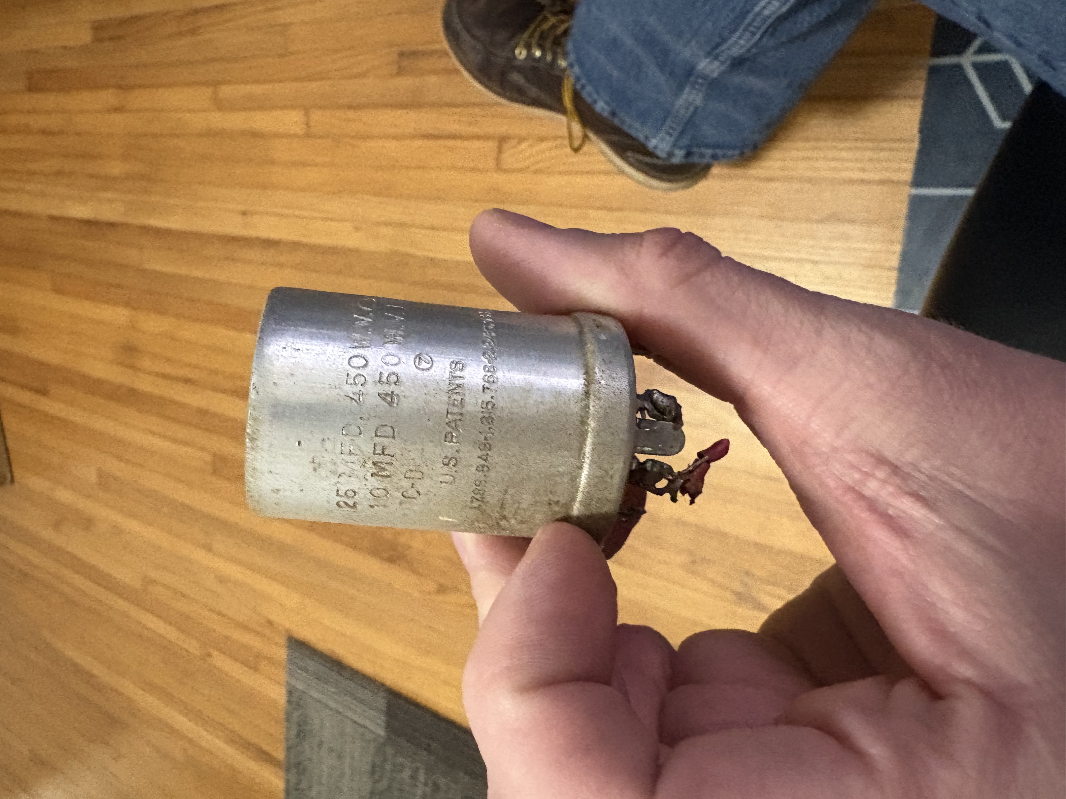
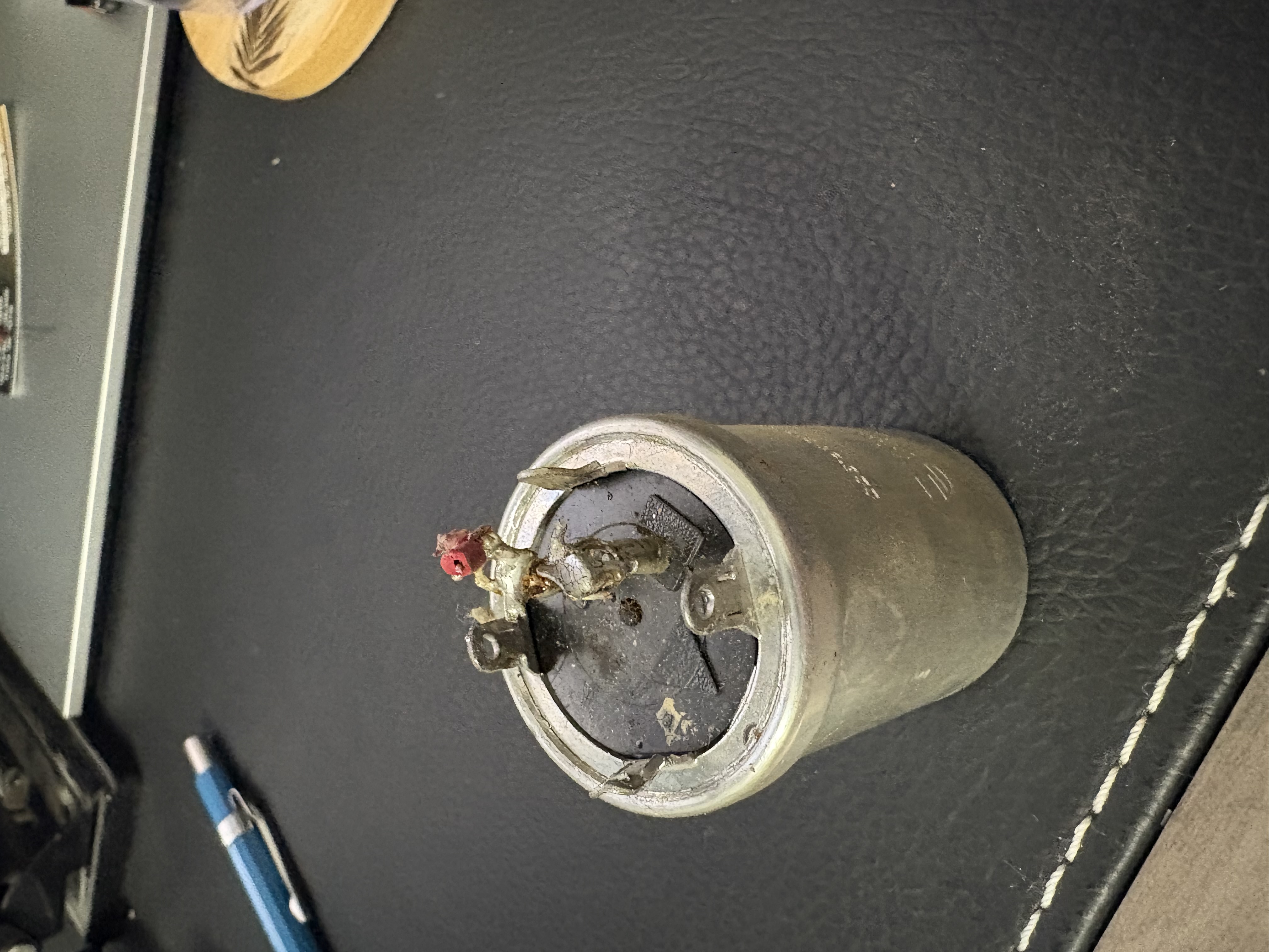
I've gotten a lot of great feedback from folks here on the Phorum. I've been worried about the high voltage (340 V) being supplied by the 7F8 rectifier. I researched into dielectrics, clearance, and creepage. As it turns out, KiCAD has some tools.
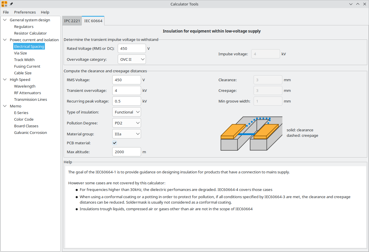
There were two tools to use, one which follows the IPC 2221 guidelines and another which follows the more stringent IEC 60664 guidelines. I chose the latter. I made some conservative assumptions in order to design for worst-case scenarios.
* Though there will only be 340 VDC, the Philco component is rated for 450 VDC. I figured I would match that, so I selected a working voltage of 450V.
* I also read online that any consumer product which is plugged into AC mains via a disconnectable plug (i.e., anything which is not hardwired) must be designed to overvoltage category 2, meaning it must be able to withstand a transient voltage of four times the working voltage. This put me in the 4kV category for transient voltage.
* I selected functional insulation, as I am not installing any further insulation on this capactitor PCB to protect the end user. This will only feature the dielectric insulation, insulation from the connected wiring, etc.
* I selected pollution degree 2. I had to research this a bit. Some folks consider residential environments to be a pollution degree 1 environment while others consider it to be pollution degree 2. I opted for the worst case scenario of pollution degree 2. Essentially, environments with pollution degree 2 may encounter higher levels of dust and/or occasional exposure to moist air.
* I selected material group IIIa. I have always used OSH Park for my PCB manufacturing, so I browsed their website for information regarding the properties of their PCB cores (datasheet attached). The CTI of their core material is specified as >175. This is the minimum for material group IIIa.
Given these assumptions, the tool determined that I need a minimum clearance of 3mm and a minimum creepage of 3mm. Simple enough! To determine the minimum trace width, I needed to know the current passing through these capacitors. I know that this is a 70 watt radio. Let's assume that the entire 70 watts passes through either one of those capacitors at 340 V. If P = V*I, then I = P/V = 70 watts / 340 V = 0.21A. Thus, the minimum trace width is just shy of 0.2mm. Mind you, the high-voltage winding of the transformer is rated to output 85mA, so this is a very conservative calculation. Even so, I had the real estate available on my PCB to make the traces a full 1.0mm wide. I had chosen a trace width of 1.0mm on the multi-section capacitor I designed for my 49-906 as well, and I've run that radio for at least 200 hours since. No issues whatsoever!.
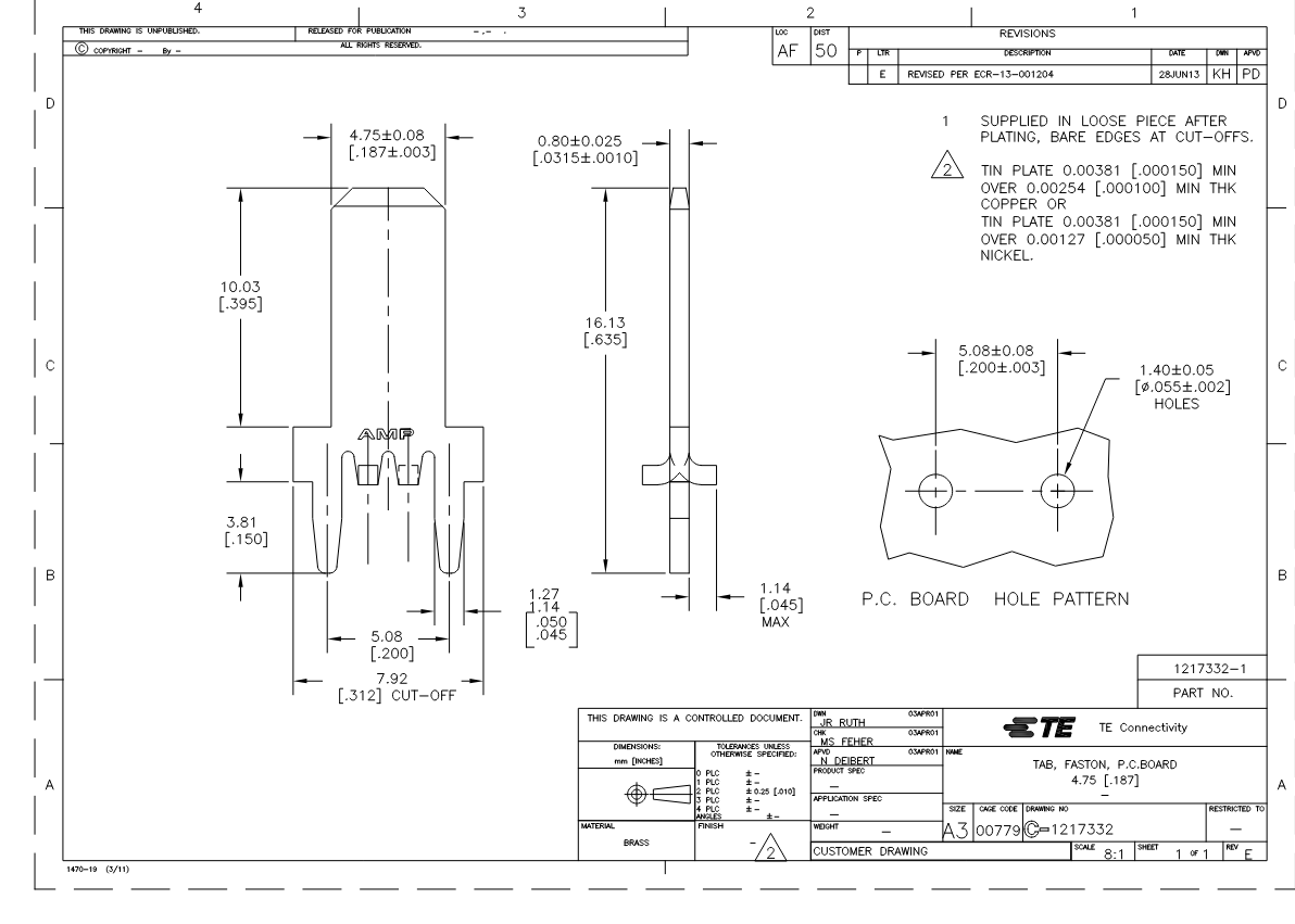
Alright, so then it was time to design the PCB. I chose these QC connectors as a close replica of the twist lock connectors (thank you to Mike for recommending those to me). As he mentioned, I can cut a notch on either side to allow for a twist after sliding through the mounting cutouts in the chassis. I chose the 0.187" wide version. The mounting cutouts on the chassis measure 0.225" wide, and these were the largest size which would fit through without being too large. Remember that these connectors serve not only as the structural mounts to the chassis, but also as the negative connections to the two capacitors. There are four of these connectors, and they are all tied to the negative terminal of both capacitors. I could not find a current rating for this connector. I did, however, find a current rating for one of the smaller versions of this connector. It was rated for 2A. Thus, I believe that this larger connector will be plenty adequate. In any event, I am very confident that it will tolerate 85mA DC.
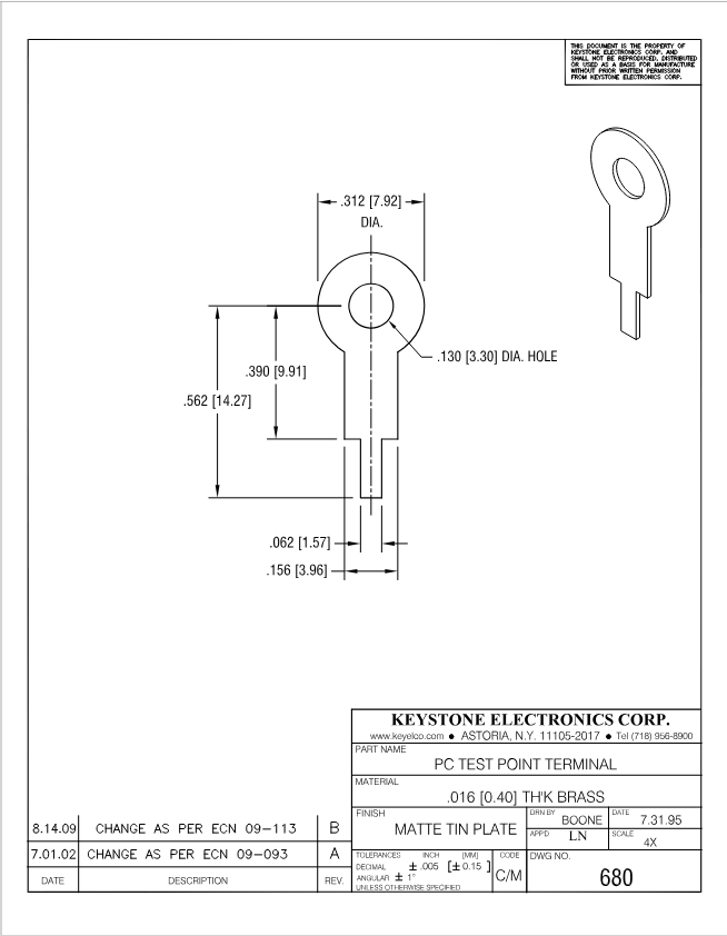
I then selected these PCB-mounted solder lugs for the positive terminal of each capacitor. Note that the two capacitors' positive terminals are not electrically connected. I could not find a current rating for this connector at all, but given the comparable sizing of this solder lug to the QC connectors I believe it should be in the same ballpark. I am also confident that this connector will tolerate 85mA DC.
Now to the capacitors. I ordered these back in late August after a discussion here on the Phorum. I have a Nichicon 10 µF, 450V, 20% electrolytic capacitor and a Nichicon 27 µF, 450V, 20% electrolytic capacitor (the original values were 10 µF and 25 µF, but I had to opt for a 27 µF replacement).
PCB footprints were available on Mouser for all but the 27µF capacitor. I was able to copy and modify the footprint for the 10 µF model, though. Lead spacing was the same. All that differed was the diameter (10mm for the 27 µF capacitor vs 12.5mm for the 10 µF capacitor).
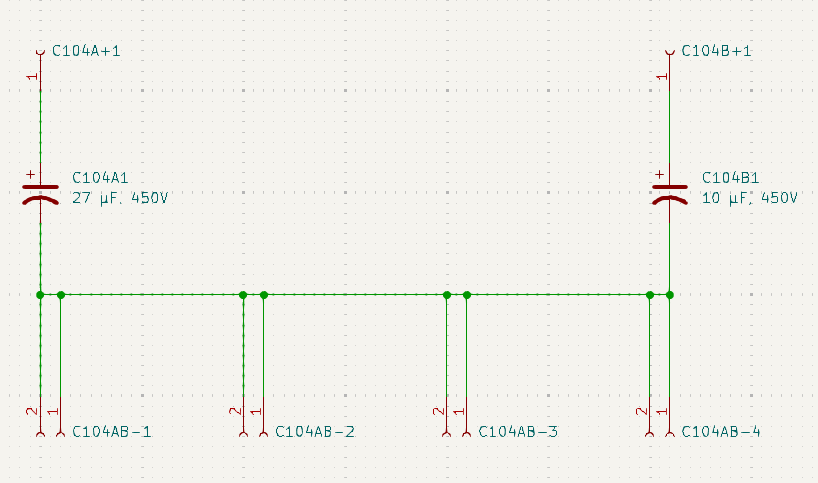
Here's a look at the schematic. It looks funny for a schematic, but bear in mind that KiCAD thinks in terms of footprints. Each of the QC connector terminals has two through-hole connectors, hence the two-socket connectors. There are also a total of four of these terminals, and that's why there are four copies on the schematic.
From there I created the PCB. Here's a glance at the wireframe design.
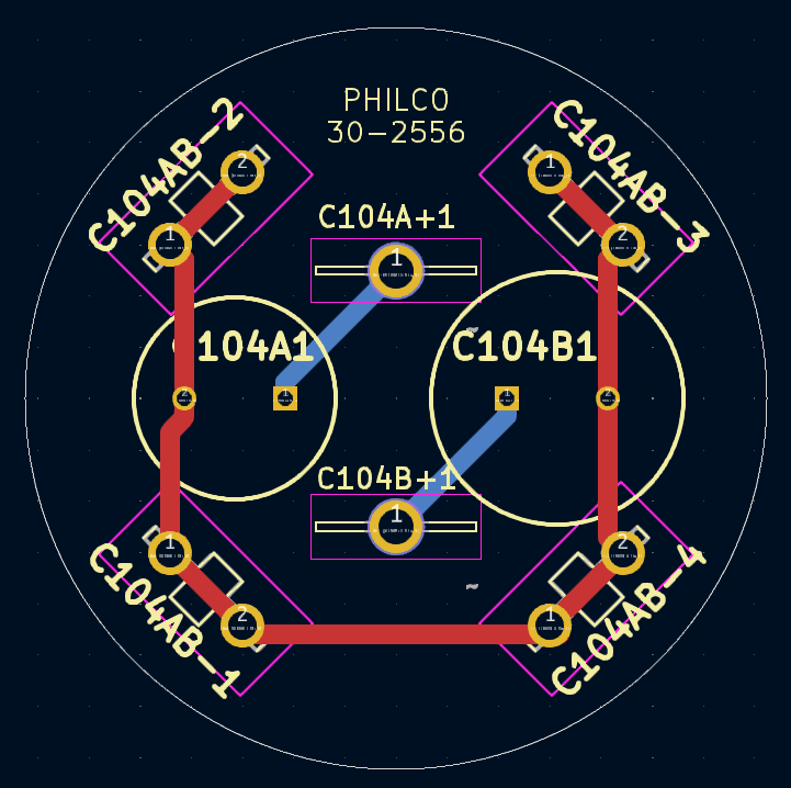
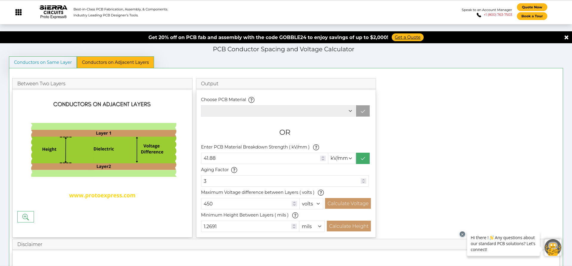
I placed all of the negative traces on the top copper trace layer (red), and the two positive traces on the bottom copper trace layer (blue). Note that there's no overlapping of these traces, but if there were then we would need to be mindful of the clearance between any two overlapping traces. According to one of the tools which OSH Park shared with me (https://designertools.app.protoexpress.com/?appid=CSCAL), the minimum separation of two traces rated for 450 V on adjacent layers would be 1.2691 mils. Here I have taken the dielectric breakdown of 67kV from the same attached datasheet. There's a note specifying that this value was calculated based upon test PCBs with an average thickness of 1.6mm, so I calculated a material breakdown strength of 41.88 kV/mm.
Per OSH Park's specifications, the core separating two layers of traces (speaking about their standard two-layer PCB) is 60 mils thick, +/- 6 mils. Thus, we are exceeding the minimum requirement of 1.2691mils of separation.
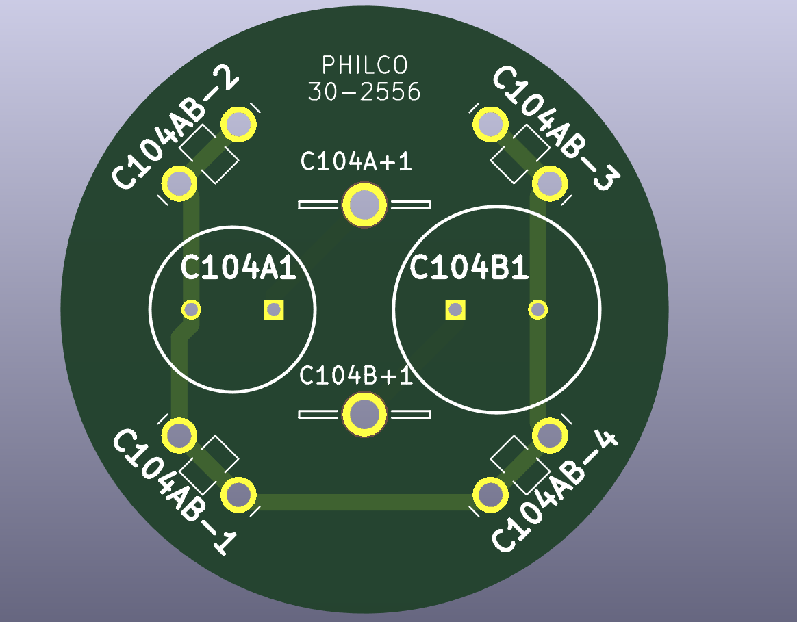
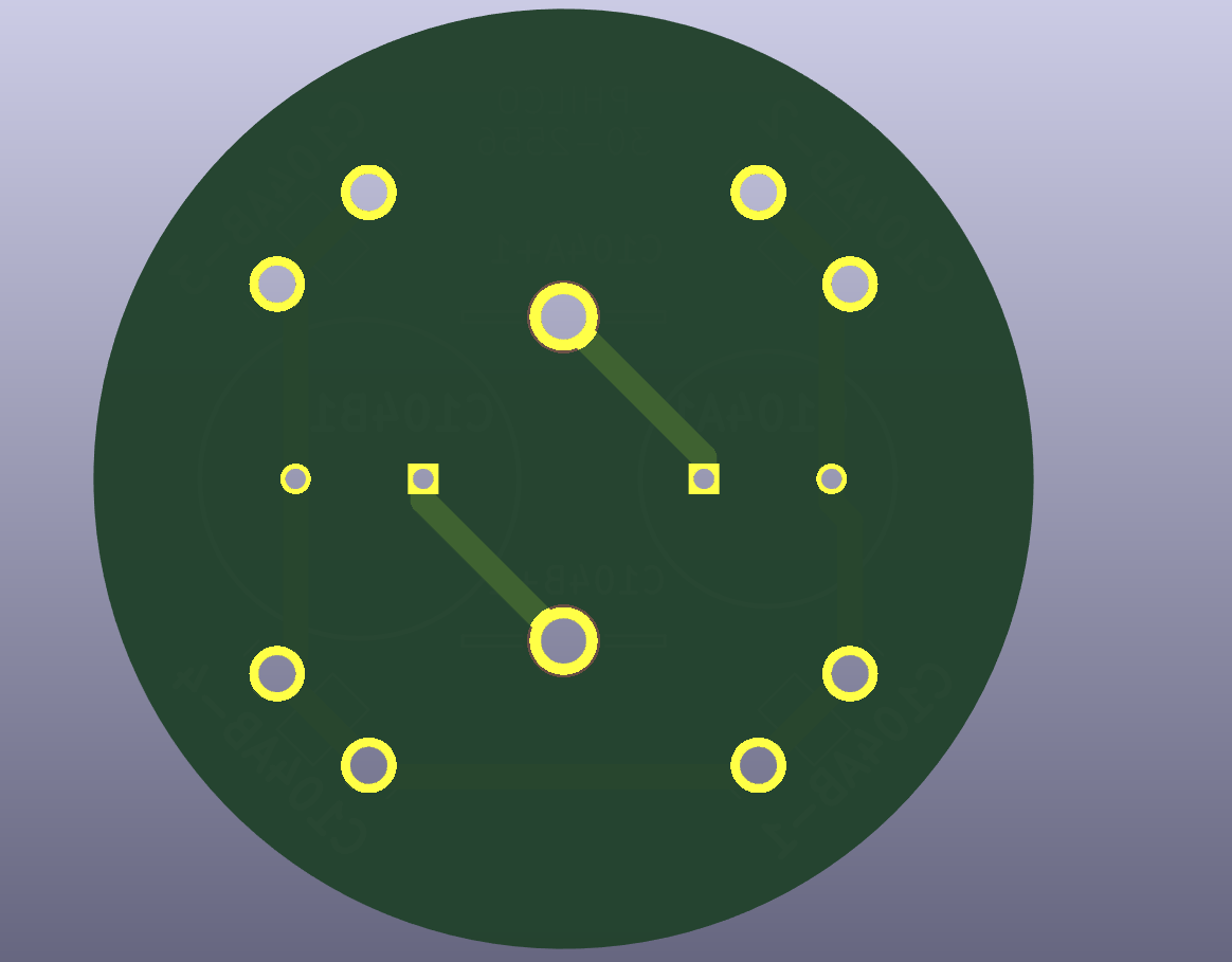
And here are the top and bottom views of the PCB from the 3D viewer tool.
I've gotten a lot of great feedback from folks here on the Phorum. I've been worried about the high voltage (340 V) being supplied by the 7F8 rectifier. I researched into dielectrics, clearance, and creepage. As it turns out, KiCAD has some tools.
There were two tools to use, one which follows the IPC 2221 guidelines and another which follows the more stringent IEC 60664 guidelines. I chose the latter. I made some conservative assumptions in order to design for worst-case scenarios.
* Though there will only be 340 VDC, the Philco component is rated for 450 VDC. I figured I would match that, so I selected a working voltage of 450V.
* I also read online that any consumer product which is plugged into AC mains via a disconnectable plug (i.e., anything which is not hardwired) must be designed to overvoltage category 2, meaning it must be able to withstand a transient voltage of four times the working voltage. This put me in the 4kV category for transient voltage.
* I selected functional insulation, as I am not installing any further insulation on this capactitor PCB to protect the end user. This will only feature the dielectric insulation, insulation from the connected wiring, etc.
* I selected pollution degree 2. I had to research this a bit. Some folks consider residential environments to be a pollution degree 1 environment while others consider it to be pollution degree 2. I opted for the worst case scenario of pollution degree 2. Essentially, environments with pollution degree 2 may encounter higher levels of dust and/or occasional exposure to moist air.
* I selected material group IIIa. I have always used OSH Park for my PCB manufacturing, so I browsed their website for information regarding the properties of their PCB cores (datasheet attached). The CTI of their core material is specified as >175. This is the minimum for material group IIIa.
Given these assumptions, the tool determined that I need a minimum clearance of 3mm and a minimum creepage of 3mm. Simple enough! To determine the minimum trace width, I needed to know the current passing through these capacitors. I know that this is a 70 watt radio. Let's assume that the entire 70 watts passes through either one of those capacitors at 340 V. If P = V*I, then I = P/V = 70 watts / 340 V = 0.21A. Thus, the minimum trace width is just shy of 0.2mm. Mind you, the high-voltage winding of the transformer is rated to output 85mA, so this is a very conservative calculation. Even so, I had the real estate available on my PCB to make the traces a full 1.0mm wide. I had chosen a trace width of 1.0mm on the multi-section capacitor I designed for my 49-906 as well, and I've run that radio for at least 200 hours since. No issues whatsoever!.
Alright, so then it was time to design the PCB. I chose these QC connectors as a close replica of the twist lock connectors (thank you to Mike for recommending those to me). As he mentioned, I can cut a notch on either side to allow for a twist after sliding through the mounting cutouts in the chassis. I chose the 0.187" wide version. The mounting cutouts on the chassis measure 0.225" wide, and these were the largest size which would fit through without being too large. Remember that these connectors serve not only as the structural mounts to the chassis, but also as the negative connections to the two capacitors. There are four of these connectors, and they are all tied to the negative terminal of both capacitors. I could not find a current rating for this connector. I did, however, find a current rating for one of the smaller versions of this connector. It was rated for 2A. Thus, I believe that this larger connector will be plenty adequate. In any event, I am very confident that it will tolerate 85mA DC.
I then selected these PCB-mounted solder lugs for the positive terminal of each capacitor. Note that the two capacitors' positive terminals are not electrically connected. I could not find a current rating for this connector at all, but given the comparable sizing of this solder lug to the QC connectors I believe it should be in the same ballpark. I am also confident that this connector will tolerate 85mA DC.
Now to the capacitors. I ordered these back in late August after a discussion here on the Phorum. I have a Nichicon 10 µF, 450V, 20% electrolytic capacitor and a Nichicon 27 µF, 450V, 20% electrolytic capacitor (the original values were 10 µF and 25 µF, but I had to opt for a 27 µF replacement).
PCB footprints were available on Mouser for all but the 27µF capacitor. I was able to copy and modify the footprint for the 10 µF model, though. Lead spacing was the same. All that differed was the diameter (10mm for the 27 µF capacitor vs 12.5mm for the 10 µF capacitor).
Here's a look at the schematic. It looks funny for a schematic, but bear in mind that KiCAD thinks in terms of footprints. Each of the QC connector terminals has two through-hole connectors, hence the two-socket connectors. There are also a total of four of these terminals, and that's why there are four copies on the schematic.
From there I created the PCB. Here's a glance at the wireframe design.
I placed all of the negative traces on the top copper trace layer (red), and the two positive traces on the bottom copper trace layer (blue). Note that there's no overlapping of these traces, but if there were then we would need to be mindful of the clearance between any two overlapping traces. According to one of the tools which OSH Park shared with me (https://designertools.app.protoexpress.com/?appid=CSCAL), the minimum separation of two traces rated for 450 V on adjacent layers would be 1.2691 mils. Here I have taken the dielectric breakdown of 67kV from the same attached datasheet. There's a note specifying that this value was calculated based upon test PCBs with an average thickness of 1.6mm, so I calculated a material breakdown strength of 41.88 kV/mm.
Per OSH Park's specifications, the core separating two layers of traces (speaking about their standard two-layer PCB) is 60 mils thick, +/- 6 mils. Thus, we are exceeding the minimum requirement of 1.2691mils of separation.
And here are the top and bottom views of the PCB from the 3D viewer tool.
Joseph
Philco 46-480
Philco 49-906


![[-] [-]](https://philcoradio.com/phorum/images/bootbb/collapse.png)


