01-11-2025, 11:08 PM
Luckily my plan is for those solder lugs to be on the underside of the PCB, whereas the capacitors will be on the top side. Even so, I know that the through-hole connector will protrude just a bit through the top. I measured, and there should be 3.4mm of clearance between the connector and the edge of the capacitor. Great consideration!
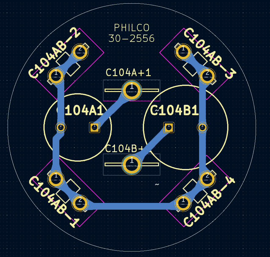
As for the comment about the high voltage traces, I hadn't considered this. You clearly have a lot of experience designing PCBs. I welcome all of these comments! Lets fix this by placing all traces on the bottom layer. All traces will be on the opposite side of the PCB compared to the capacitors. The traces connecting to the negative contacts will be equipotential with the chassis, so it wouldn't matter if the solder mask were scraped and the trace contacted the chassis. Additionally, the two positive contacts could not possibly touch the chassis as they are located in the area of the cutout in the chassis.

As for the comment about the high voltage traces, I hadn't considered this. You clearly have a lot of experience designing PCBs. I welcome all of these comments! Lets fix this by placing all traces on the bottom layer. All traces will be on the opposite side of the PCB compared to the capacitors. The traces connecting to the negative contacts will be equipotential with the chassis, so it wouldn't matter if the solder mask were scraped and the trace contacted the chassis. Additionally, the two positive contacts could not possibly touch the chassis as they are located in the area of the cutout in the chassis.
Joseph
Philco 46-480
Philco 49-906


![[-] [-]](https://philcoradio.com/phorum/images/bootbb/collapse.png)


