01-12-2025, 12:21 PM
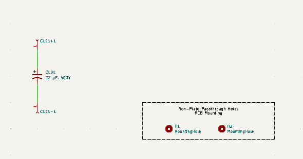
I started this morning on the design for a PCB for C101. The original component is a single-section electrolytic capacitor mounted on a phenolic wafer. C101 is a 22 µF, 450 VDC, 20% capacitor. I began with the schematic. Again, KiCAD is strange because you have to add any mounting holes to the schematic. But here it is.

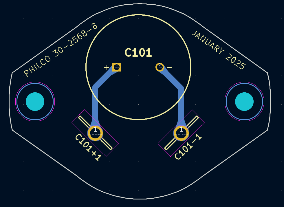
I am using the same solder lugs as I used for C104 A/B, so I imported the same footprint library. I also was able to get this capacitor's footprint from Mouser's website. I paired footprints to schematic symbols, and then started with the PCB design. I borrowed the shape of this PCB from the design I created for my 49-906 multi-section capacitor. I utilized the tips Mike provided for my C104 A/B capacitor, and applied them here (traces on the opposite side of the PCB if they cross the edge of the capacitor's can, adding teardrops to the through-hole mounts, etc.). I've also used the same clearance, creepage, and ampacity assumptions I made for C104 A/B. My traces are 1mm wide and I'm assuming a minimum clearance and creepage of 3mm. All clearances and creepages for through-hole connectors and traces are acceptable on this board. I also temporarily inserted a ring to represent the circle cutout on the chassis. All connectors are at least 3mm away from the cutout, so there will be no clearance issues with the chassis. The only comment I will make is that the capacitor's can is not 3mm away from the upper edge of the PCB. I simply did not have enough space on this PCB to make that happen. However, we are not assuming that the body of the capacitor is energized. Here's a snapshot of this PCB.

I added the date to this PCB. I had forgotten to add that to the PCB for C104 A/B, but I will do that now. It will help me remember 15 years from now that it's time to recap this radio!
I am using the same solder lugs as I used for C104 A/B, so I imported the same footprint library. I also was able to get this capacitor's footprint from Mouser's website. I paired footprints to schematic symbols, and then started with the PCB design. I borrowed the shape of this PCB from the design I created for my 49-906 multi-section capacitor. I utilized the tips Mike provided for my C104 A/B capacitor, and applied them here (traces on the opposite side of the PCB if they cross the edge of the capacitor's can, adding teardrops to the through-hole mounts, etc.). I've also used the same clearance, creepage, and ampacity assumptions I made for C104 A/B. My traces are 1mm wide and I'm assuming a minimum clearance and creepage of 3mm. All clearances and creepages for through-hole connectors and traces are acceptable on this board. I also temporarily inserted a ring to represent the circle cutout on the chassis. All connectors are at least 3mm away from the cutout, so there will be no clearance issues with the chassis. The only comment I will make is that the capacitor's can is not 3mm away from the upper edge of the PCB. I simply did not have enough space on this PCB to make that happen. However, we are not assuming that the body of the capacitor is energized. Here's a snapshot of this PCB.
I added the date to this PCB. I had forgotten to add that to the PCB for C104 A/B, but I will do that now. It will help me remember 15 years from now that it's time to recap this radio!
Joseph
Philco 46-480
Philco 49-906


![[-] [-]](https://philcoradio.com/phorum/images/bootbb/collapse.png)


