A thought came to my mind as I arose Sunday morning (March 28). What about that section of wafer C that grounds the wiper arm of the bass control on all bands save for Band 1? I resolved to check into that as soon as I could.
On Monday, March 29, I lifted the ground wire from switch contact C11 and voila, there was no more partial short to ground from contact C4, C8, C9 or C12 to the metal plate. So, a carbon track is definitely indicated. I measured resistance from contact C11 to C4, C8, C9 and C12. Yes, similar resistances as posted in my blog post of Monday, March 29 were still showing. I have traced the issue down to the defective part, and it is switch wafer C.
Now the question was, What can I do about it? I have these two RF units in the parts box which the radio’s owner brought here, along with the entirety of the 38-690 chassis. I had tested both switch wafer Cs from both parts units and they passed (no shorts to ground in the suspect areas). However, simply replacing one wafer for another is not going to guarantee a permanent solution. I need to come up with a way to avoid having high voltage B+ and ground potential on the same wafer.
First of all – the bass control shorting. Why did Philco design this so that the bass control’s wiper arm would be shorted out, rendering the control ineffective, on all bands except Band 1 (the standard AM band)? I can only guess, and my guess is that David Grimes and his team at Philco felt that heavy fading and other propagation issues on shortwave might tend to overload the woofer at times, so they devised a quick and easy way to defeat the bass control on all bands except Band 1.
It would have been fine…EXCEPT this places B+ and ground potential in very close proximity to one another, so close that it would be quite easy for a spark to jump from B+ to ground, and a carbon track to begin to form. This is what happened to the subject 38-690. I am frankly amazed that this has not happened to more 38-690 sets. Perhaps it did happen to some 38-690 sets which have not survived – the carbon track was formed, and the radio was then declared unrepairable by a repairman, and thus disposed of.
Secondly – Philco, for ease of manufacture, chose to ground all five of the RF coil secondaries through convenient (for them) tie points at terminals C3 and C5. This gave those coil secondaries a connection to ground through contact C11, which was wired to the metal plate and, therefore, ground. C11 is always at ground potential and is tied to a thin ring on the movable portion of the switch wafer. This goes around one side of switch wafer C, also contacting C10, C3 and C5.
To get a better idea of this, let us take a look at a drawing of switch wafer C, from the schematic:
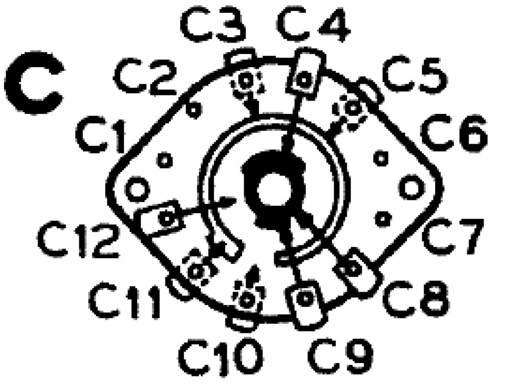
38-690 Switch Wafer C.
In the drawing above, terminals C4, C8, C9 and C12 all connect to B+, depending upon the setting of the band switch. At the same time, terminals C3, C5, C10 and C11 connect to chassis ground – again, depending upon the setting of the band switch. The construction of the band switch is such that a high B+ voltage (the 38-690 service information does not give voltages) and chassis ground potential is right there, side by side, within a fraction of an inch of each other!
This gives me even more reason to wish I could bring David Grimes back so I could slap him around multiple times and kick him a few times as well. He deserves it! This is terrible, actually stupid, design work. There was no good reason for doing this other than simply taking the easy way out.
A brief background on David Grimes: He first came into prominence in the mid-1920s with his “Inverse Duplex” radios. These used a reflex circuit whereby the RF tubes were also used in turn for audio amplification. His “David Grimes Radio Co.” did not last very long, and he later worked for RCA before being hired by Philco as their Chief Engineer. Philco had always cut corners wherever they could in their set design, so Grimes was apparently a “good fit” for Philco. While Grimes was Chief Engineer, Philco’s radios gradually became of lesser quality as Grimes cut even more corners – such as this switch wafer C in the 38-690 and 38-116 Code 125.
Anyway –
The partial schematic below illustrates what I am talking about, with my proposed changes in orange.
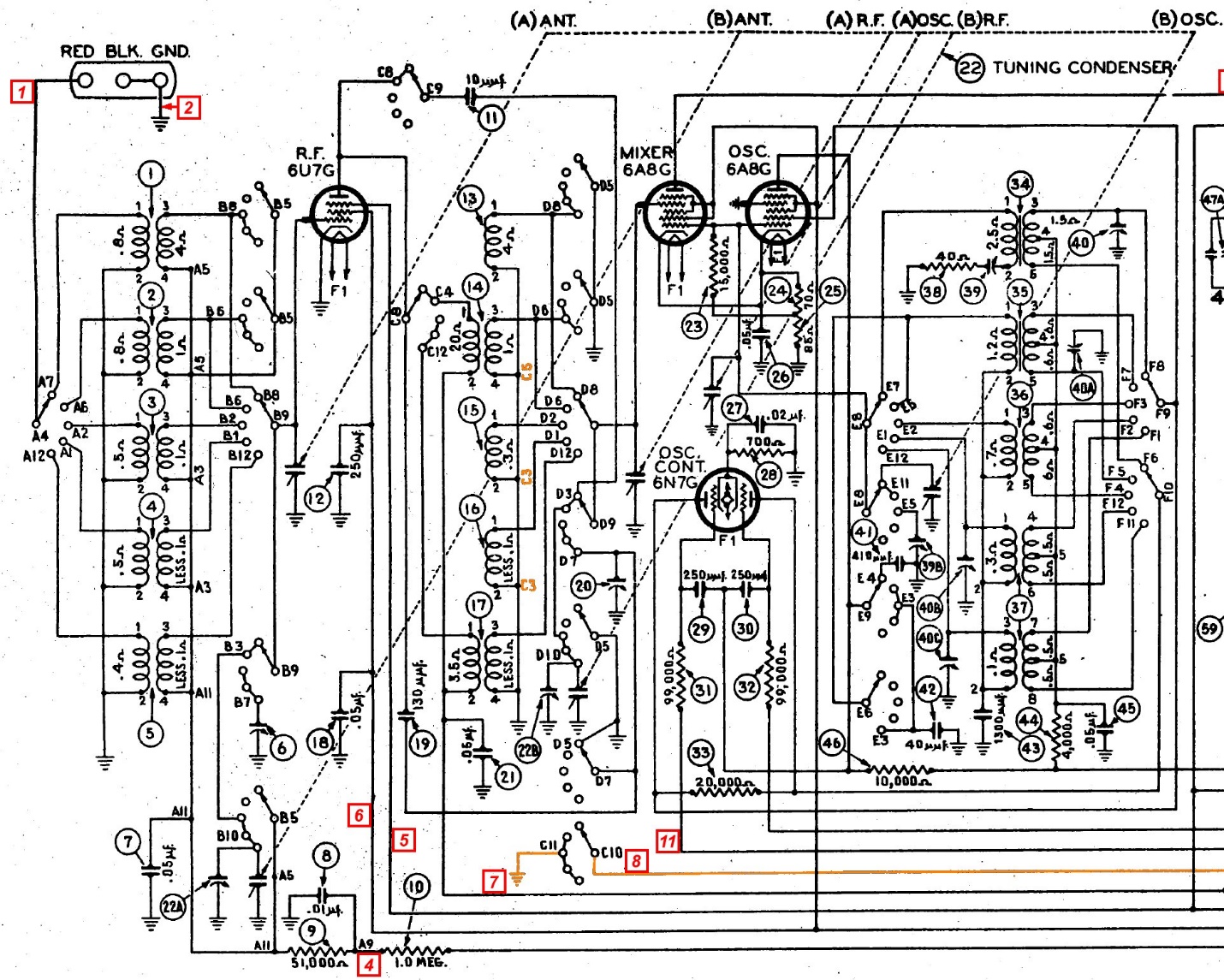
Proposed changes to 38-690 circuitry to eliminate any possibility of B+ to ground shorts in switch wafer C.
To permanently eliminate the trouble of having ground potential too close to B+ and on the same switch wafer, we need to make some modifications.
The bass control shorting is not necessary. Now that these old radios are mostly in the hands of dedicated collectors and not the general public, most radio collectors have enough sense not to crank the bass control to full blast on shortwave. So, I will eliminate that shorting “feature”. Switch terminals C10 and C11 will no longer be connected to anything. This, in turn, will completely eliminate wire [8] from the RF unit.
We can also change how the RF coils are grounded, by tying those coil leads which formerly connected to terminals C3 and C5 to switch wafer D, terminal D5, instead. I will do this by lengthening the leads of each coil lead as needed, with small gauge stranded wire which will be insulated as appropriate, and soldering each to terminal D5. Another wire will run from D5 to the ground point on the metal plate. This will fully eliminate the extreme close proximity of B+ and ground potential on switch wafer C – in fact wafer C will only be switching the primaries of RF coils (14) and (17), as well as switching 10 pF mica capacitor (11) in and out of the circuit, and nothing more.
The following partial schematic shows how things will look after these changes are made:
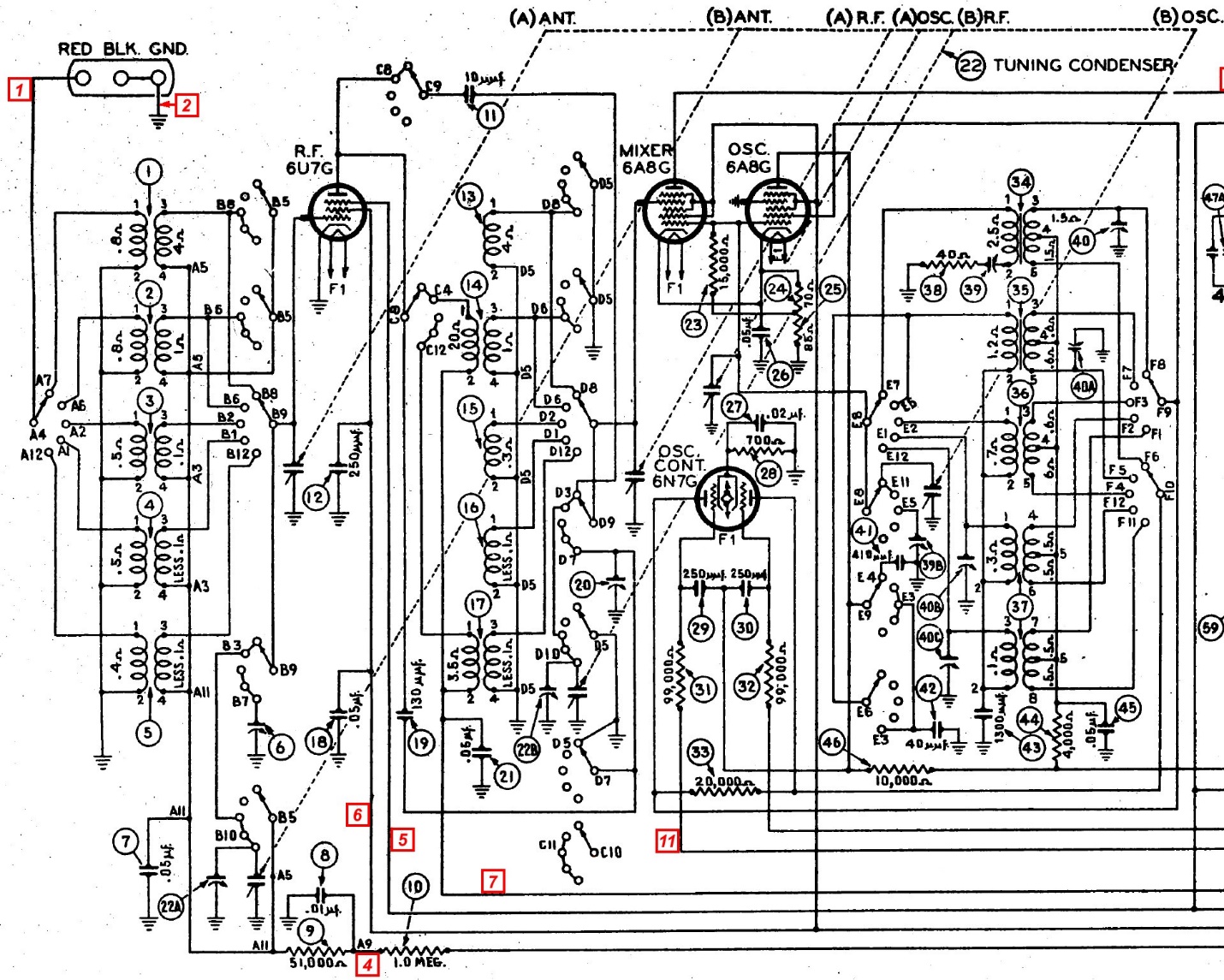
How the 38-690 circuitry will look after the changes have been made.
Notice there is nothing connected to switch terminals C10 or C11…or C3, or C5 for that matter. Also, lead 2 of coils (13), (15) and (16), and lead 4 of coils (14) and (17), will now all connect to switch terminal D5 on switch wafer D. A wire from D5 will go to a ground terminal on the RF section. Thus, there will be nothing on switch wafer C that will be connected to ground potential and, therefore, there will be no chance of B+ leaking to ground on that wafer.
This is the new plan of attack. I see no reason why it will not be successful.
Next time, I will put these plans into action by disassembling the RF section as I did with the three sections of the 37-116 RF unit. After disassembly, I will see if I can find the carbon track and then determine if it is repairable. If not, I have two more switch wafers I can use, and I will use one of them if necessary. So, stay tuned – things are definitely looking up now!